
 Product
 Brand
Brand Articles
 Tools
Tools
What is Comparator?
Comparator Explained (Inverting Comparator, Non-Inverting Comparator and Window Comparator)
| Topics covered in this article: |
| Ⅰ. What is a voltage comparator? |
| Ⅱ. How does comparator work? |
| Ⅲ. Difference between comparator and op amp |
| Ⅳ. Comparator typical application circuit |
A voltage comparator (also known as a comparator) is a very common integrated circuit. It can be utilized in V/F conversion circuits, A/D conversion circuits, high-speed sampling circuits, power supply voltage monitoring circuits, oscillators and voltage-controlled oscillator circuits, and zero-crossing detection circuits, among other things. This page focuses on the fundamental concept, working principle, and typical working circuit of voltage comparators, as well as some often used voltage comparators.
Ⅰ. What is a voltage comparator?
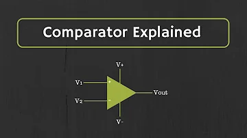
Simply put, the voltage comparator analyzes the magnitude of two analog voltages (there are also two digital voltages for comparison, but they will not be discussed here) and determines which has the larger voltage, as illustrated in Figure 1. Figure 1(a) depicts a comparator with two input terminals: a non-inverting ("+") and an inverting ("-") input terminal, as well as an output terminal Vout (output level signal). The power supply V+ and ground (this is a single power supply comparator), the non-inverting terminal input voltage VA, and the inverting terminal input VB are also present. Figure 1 depicts the changes in VA and VB (b). VA>VB during time 0-t1; VB>VA during time t1-t2; VA>VB during time t2-t3. Figure 1(c) shows the output of Vout in this case: When VA>VB, Vout produces a high level of output (saturated output); when VB>VA, Vout produces a low level of output. You can tell which voltage is greater by looking at the output level.

Figure. 1
When VA is applied to the inverting terminal and VB to the non-inverting terminal, the voltage changes of VA and VB remain the same as in Figure 1(b), and the Vout output remains the same (d). The output level is inverted in comparison to Fig. 1(c). The input terminals of VA and VB are related to the output level change together.
Figure 2(a) shows a comparator with two power supplies (positive and negative power supplies). Figure 1(b) shows the output characteristic of a VA, VB input voltage. Figure 2 shows the output characteristic of a VA, VB input voltage (b). Vout outputs a saturated negative voltage when VB>VA.

Figure. 2
As indicated in Figure 3, the input voltage VA is compared to a fixed voltage VB (a). This VB is referred to as the reference voltage, threshold voltage, or reference voltage. This reference voltage is typically employed for zero-crossing detection if it is 0V (ground level), as shown in Figure 3(b).

Figure. 3
Ⅱ. How does comparator work?
The comparator is derived from the operational amplifier, and the comparator circuit can be thought of as an operational amplifier application circuit. Special comparator integrated circuits have been developed due to the widespread use of comparator circuits.
The input voltage VA is split by the voltage divider R2, R3 and then connected to the non-inverting terminal, VB is connected to the inverting terminal by the input resistor R1, and RF is the feedback resistor in Figure 4(a). The output voltage Vout, VA, VB, and the four resistors have the following connection when considering the input offset voltage: Vout=(1+RF/R1)〃R3/(R2+R3)VA-(RF/R1)VB. If R1=R2, R3=RF, Vout=RF/R1(VA-VB), where RF/R1 is the amplifier gain. Vout= when R1=R2=0 (equivalent to R1, R2 short circuit), R3=RF= (equivalent to R3, RF open circuit), and R3=RF= (equivalent to R3, RF open circuit). Figure 4 shows the circuit diagram for when the gain becomes infinite (b). The comparator circuit, which is the differential amplifier, is in an open-loop state. In actuality, the op amp's gain is not infinite in the open loop condition, and the Vout output is the saturation voltage, which is smaller than the positive and negative supply voltages and cannot be infinite.

Figure. 4
The comparator circuit is a differential amplifier circuit in which the operational amplifier circuit is in an open-loop state, as shown in Figure 4.
Figure 5 depicts a non-inverting amplifier circuit. If RF= in Fig. 5 and R1=0, the comparator circuit is the same as in Fig. 3. (b). In Figure 5, Vin corresponds to VA in Figure 3. (b).

Figure. 5
Ⅲ. Difference between comparator and op amp
Comparator circuits can be made with op amps, however superior performance comparators offer higher open-loop gain, smaller input offset voltages, larger common-mode input voltage ranges, and faster slew rates than general-purpose op amps (making the comparators respond faster). Furthermore, the comparator's output stage normally has an open-collector layout, as shown in Figure 6, which requires an external pull-up resistor or direct driving of loads with varying power supply voltages, making it more adaptable in application. However, there are complementary output comparators that do not require pull-up resistors.

Figure. 6
It should be noted, however, that the comparator circuit has technical criteria as well, including accuracy, reaction speed, propagation delay time, sensitivity, and so on. The majority of the parameters are the same as the op amp. A general-purpose op amp can be utilized as a comparator circuit when the criteria are not stringent. In the A/D converter circuit, for example, a precise comparator circuit is required.
Because the internal structure of the comparator and the op amp is almost the same, the majority of its parameters (electrical characteristic parameters) are nearly identical to the op amp's parameter items (such as input offset voltage, input offset current, and input bias current, etc.).
Ⅳ. Comparator typical application circuit
Here are two simple comparator circuits as examples to illustrate their applications.
1. Cooling fan automatic control circuit
Some high-power devices or modules will generate additional heat during operation in order to raise the temperature. To maintain normal operation, heat sinks and fans are typically utilized to cool them. As shown in Figure 7, a very simple temperature control circuit is introduced. To detect the temperature of the power device, a negative temperature coefficient (NTC) thermistor RT is pasted on the heat sink (the temperature on the heat sink is slightly lower than the temperature of the device). There is a voltage VA when 5V is applied to the RT and R1 resistors. The resistance of the thermistor RT decreases as the temperature of the heat sink rises, causing VA to rise. Figure 8 depicts the temperature characteristics of RT. It is a single-valued function, despite the fact that its resistance and temperature change curves are not linear (that is, when the temperature is constant, its resistance value is also a certain single-valued). The cooling fan should be turned on if the temperature is set to 80°C. The set threshold temperature TTH is 80°C, and the characteristic curve shows the resistance value of RT corresponding to 80°C. The VA value at 80°C may be determined if the resistance value of R1 remains unchanged (it is installed on the circuit board, and the value of R1 can be considered unchanged when the ambient temperature changes slightly).

Figure. 7
A voltage divider is formed by R2 and RP. Adjusting RP can affect the voltage of VB when the 5V power supply voltage is stable (excellent voltage stability) (the voltage value of the potentiometer center head). The threshold voltage set by the comparator, called VTH, is the VB value.
When designing, it is desired that once the heat sink temperature surpasses 80 °C, the cooling fan will be activated to achieve heat dissipation, and the value of VTH will be equal to the K value at 80 °C. The comparator outputs a low signal when VA>VTH, the relay K pulls in, and the cooling fan (DC motor) is powered to cool the high-power device. Figure 8 depicts the properties of VA, VTH voltage variation, and comparator output voltage Vout. It should be noted that when VA exceeds VTH, the fan activates, but the heat sink retains a significant amount of heat, and it takes some time to drop the temperature to below 80°C.

Figure. 8
It is highly convenient to adjust the threshold temperature TTH, as shown in FIG. 7, as long as the VTH value is modified as well. When the VTH value rises, the TTH rises as well; vice versa, the adjustment is quite simple. R1, R2, and RP can be easily derived once RT and the temperature parameters of RT have been determined (set the currents flowing through RT, R1, R2, and RP to be 0.1 to 0.5 mA respectively).
2. Window Comparator
The window comparator is usually made up of two comparators (dual comparator), each of which has two threshold voltages: VTHH (high threshold voltage) and VTHL (low threshold voltage), and the voltage VA are compared to the two threshold voltages. Vout outputs a high level if VTHLVAVTHH is true; if VAVTHH is true, Vout outputs a low level, as seen in Figure 10. A refrigerator alarm circuit is shown in Figure 9. The refrigerator's regular working temperature is set to 0 to 5°C (0°C to 5°C is a "window"). The comparator outputs a high level (showing that the temperature is normal) within this temperature range; if the refrigerator temperature is below 0V or above 5°C, the comparator outputs a low level, and the low level signal voltage is supplied to the microcontroller (C) as an alert signal.

Figure. 9
NTC thermistor RT is used as the temperature sensor. At 0°C, RT has a resistance of 333.1k while at 5°C, it has a resistance of 258.3k. It is roughly 1.5 uA, based on the working voltage of 1.5V and the current flowing through R1 and RT. R1's value should be determined. After determining the value of R1, the VA value at 0°C may be computed as 0.5V (where R1=665k in Figure 9) and the VA value at 5°C can be calculated as 0.42V, resulting in VTHL=0.42V and VTHH=0.5V. Figure 10 shows the current I=(1.5V-0.5V)/665k=0.0015mA flowing through the resistors R2, R3, and R4 when R2=665k is used. R4=280k may be acquired by pressing 0.5V=(R3+R4)0.0015mA and then R3=53.3k can be obtained by pressing R4I/=0.42V.

Figure. 10
The LT1017, a low-voltage, low-power, complementary-output dual-comparator with no external pull-up resistors, is used in this application.
 UTMEL
UTMEL
We are the professional distributor of electronic components, providing a large variety of products to save you a lot of time, effort, and cost with our efficient self-customized service. careful order preparation fast delivery service
1. What is a zero-crossing comparator?
A zero-crossing comparator is a comparator that toggles the threshold to zero. The comparator is essentially an error amplifier that works in an open-loop state. It is bounded by a threshold. If it is less than the threshold, it outputs a logic. If it is greater than the threshold, it outputs the opposite logic to achieve the purpose of distinguishing the comparison results.
2. How to distinguish between amplifiers and comparators?
The difference is as follows:
1. The flip speed of the comparator is fast, about the order of ns, while the flip speed of the op amp is generally of the order of us (special high
except for high-speed op amps).
2. The op amp can be connected to a negative feedback circuit, while the comparator cannot use negative feedback.
3. The output stage of the operational amplifier generally adopts a push-pull circuit with bipolar output. However, most comparator output stages are open-collector structures.
3. What does a voltage comparator do?
Basically a voltage comparator is an A/D converter, but this A/D converter has only one bit output. The voltage comparator has two input terminals. When the voltage of the input terminal A is constant (called the reference voltage Vref), if the voltage of the other input terminal B is higher than Vref, the output terminal is high level 1, and the input terminal If the B voltage is lower than Vref, the output terminal is low level 0.
Of course, if the input terminal B is set as the reference voltage and the input terminal A is used for the voltage test, the change of the output voltage will be opposite. Using this feature, a voltage comparator can be used to detect changes in voltage and then control the switching of a circuit.
 Discovering New and Advanced Methodology for Determining the Dynamic Characterization of Wide Bandgap DevicesSaumitra Jagdale15 March 20242617
For a long era, silicon has stood out as the primary material for fabricating electronic devices due to its affordability, moderate efficiency, and performance capabilities. Despite its widespread use, silicon faces several limitations that render it unsuitable for applications involving high power and elevated temperatures. As technological advancements continue and the industry demands enhanced efficiency from devices, these limitations become increasingly vivid. In the quest for electronic devices that are more potent, efficient, and compact, wide bandgap materials are emerging as a dominant player. Their superiority over silicon in crucial aspects such as efficiency, higher junction temperatures, power density, thinner drift regions, and faster switching speeds positions them as the preferred materials for the future of power electronics.
Read More A Comprehensive Guide to FPGA Development BoardsUTMEL11 September 202520005
This comprehensive guide will take you on a journey through the fascinating world of FPGA development boards. We’ll explore what they are, how they differ from microcontrollers, and most importantly, how to choose the perfect board for your needs. Whether you’re a seasoned engineer or a curious hobbyist, prepare to unlock new possibilities in hardware design and accelerate your projects. We’ll cover everything from budget-friendly options to specialized boards for image processing, delve into popular learning paths, and even provide insights into essential software like Vivado. By the end of this article, you’ll have a clear roadmap to navigate the FPGA landscape and make informed decisions for your next groundbreaking endeavor.
Read More 800G Optical Transceivers: The Guide for AI Data CentersUTMEL24 December 20259967
The complete guide to 800G Optical Transceiver standards (QSFP-DD vs. OSFP). Overcome supply shortages and scale your AI data center with Utmel Electronic.
Read More The 2026 Engineer’s Guide: Choosing the Right MCU for Your Next IoT & New Energy ProjectUTMEL30 April 2026667
A comprehensive comparison of 2026's leading MCUs from ST, NXP, and Microchip across power efficiency, processing performance, connectivity, and ecosystems to help engineers select the optimal chip for next-gen IoT and new energy projects.
Read More AI Server Components: Engineering Next-Gen Data Center Hardware for 100kW RacksUTMEL15 May 2026370
The transition from traditional enterprise IT to AI-driven workloads has rendered legacy data center hardware obsolete, forcing infrastructure planners to re-engineer server components for extreme thermal environments.
Read More
Subscribe to Utmel !
![80HCPS1432CRM]() 80HCPS1432CRM
80HCPS1432CRMRenesas Electronics America Inc.
![SI8261BBD-C-IS]() SI8261BBD-C-IS
SI8261BBD-C-ISSilicon Labs
![SI8261BAD-C-IS]() SI8261BAD-C-IS
SI8261BAD-C-ISSilicon Labs
![FOD8333]() FOD8333
FOD8333ON Semiconductor
![FOD8332R2]() FOD8332R2
FOD8332R2ON Semiconductor
![ACPL-302J-500E]() ACPL-302J-500E
ACPL-302J-500EBroadcom Limited
![SI8275GB-IS1]() SI8275GB-IS1
SI8275GB-IS1Silicon Labs
![SI8238AD-D-IS3]() SI8238AD-D-IS3
SI8238AD-D-IS3Silicon Labs
![FOD3120SD]() FOD3120SD
FOD3120SDON Semiconductor
![ADUM3223BRZ]() ADUM3223BRZ
ADUM3223BRZAnalog Devices Inc.


